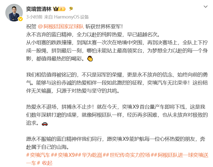
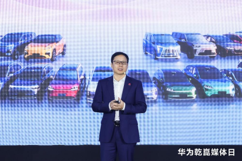
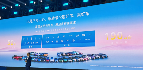
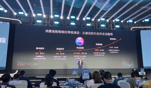
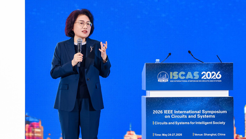
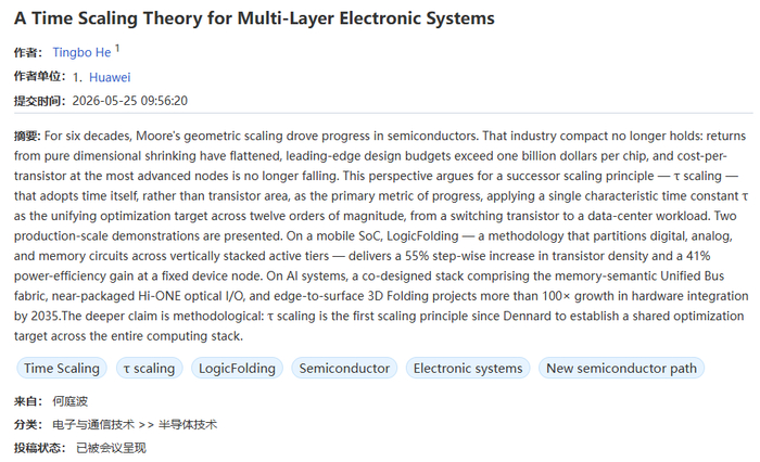
He Tingbo from Huawei delivered a keynote speech titled "New Semiconductor Path in Practice". Credit: Huawei Understand China EV’s Market Real-time notifications when critical EV data is released All important data in one place 2,000,000+ data points Become a member At the 2026 IEEE International Symposium on Circuits and Systems (ISCAS) held on May 25, He Tingbo, Director of Huawei and President of its semiconductor business, delivered a keynote titled “New Semiconductor Path in Practice.” During the address, she introduced the Tau (τ) Scaling Law, a new guiding principle designed to sustain the evolution of semiconductors as traditional Moore’s Law faces mounting physical and economic barriers. A shift from space to time For over five decades, the industry has relied on geometric scaling – shrinking transistor sizes to boost performance. However, with advanced nodes now exceeding 1 billion USD per chip in design costs and transistor cost-reduction stalling, Huawei argues that the focus must shift from “space” to “time.” The Tau Scaling Law proposes using the time constant (τ) – representing signal propagation delay – as the core metric for progress across the entire computing stack, from individual transistors to massive data centres. By systematically compressing τ, Huawei aims to drive performance and density without relying solely on the latest lithography equipment. The paper on Time Scaling. LogicFolding: revolutionising mobile SoCs A cornerstone of this new law is LogicFolding, a design methodology that stacks digital, analogue, and memory circuits into vertical active layers. In mobile SoC applications, this technology has already demonstrated a 55% leap in transistor density and a 41% improvement in energy efficiency on fixed process nodes. Huawei revealed an ambitious roadmap for its Kirin processors: 2026: The first Kirin chips to adopt LogicFolding will feature a CPU performance core frequency of 3.1 GHz. 2027-2028: Frequencies are expected to climb to 3.39 GHz and 3.71 GHz, respectively. 2029: CPU frequencies are projected to break the 4 GHz barrier. By 2031, Huawei expects its high-end chips based on the Tau Scaling Law to achieve a transistor density equivalent to a 1.4 nm (14 Å) process. Scaling AI systems The Tau Scaling Law also addresses the “fan-out dilemma” in AI computing, where memory and power delivery are limited by the chip’s perimeter. Through 3D Folding, Huawei is moving these resources to the chip’s surface, allowing them to scale with area rather than just circumference. Key AI infrastructure technologies include: UnifiedBus (UB): A protocol that reduces end-to-end remote access latency from tens of microseconds to approximately 100 nanoseconds. Hi-ONE: A high-density optical interconnect engine providing 8 Tb/s bandwidth. It reduces SerDes transmission distances from roughly 0.001 km to 0.00005 km, while extending panel-to-panel reach to 0.1 km. The Ascend 950 (2026) and Ascend 990 will initially use 2.5D and 3D stacking, with the Ascend 990 expected to fully integrate LogicFolding by 2030. A call for global collaboration He Tingbo noted that Huawei has already mass-produced 381 chips based on these principles over the last six years. However, she emphasised that the future of the semiconductor industry depends on openness. “No single company can independently find all the answers,” she stated, inviting global scientists and engineers to collaborate on the Tau Scaling Law to drive hardware integration growth by over 100 times by 2035.



















 +9 others