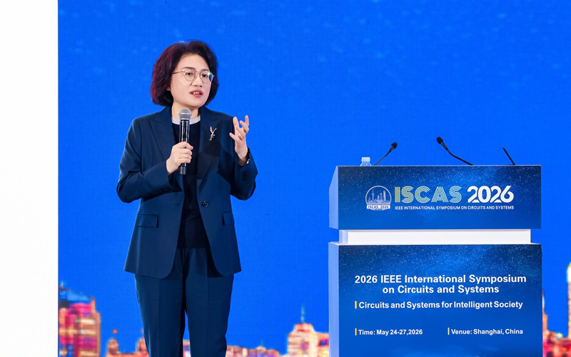
Gasgoo Munich- On May 25, industry outlet Gasgoo reported that at the 2026 International Symposium on Circuits and Systems, He Tingbo—a Huawei director and president of the company’s semiconductor business unit—formally unveiled the "Tao (τ) Law" during a keynote speech titled "Exploration and Practice of New Semiconductor Paths."Notably, this marks the first time China has proposed a new guiding principle for the development of the global semiconductor industry.Image Source: Huawei Official WebsiteThe Tao (τ) Law proposes replacing "geometric scaling" with "time (τ) scaling" as the new guiding principle for the evolution of semiconductors and electronic systems. By leveraging innovations such as logic folding, the approach aims to continuously compress signal propagation delays and boost transistor density, ensuring the steady advancement of semiconductor technology.Moore's Law has dominated the semiconductor industry for over half a century, but it is now facing severe challenges from both physical limits and diminishing economic returns. With geometric scaling slowing and cost benefits fading, the global industry faces a common dilemma: how to bypass the constraints of traditional process nodes and find a sustainable path forward to meet exponentially rising computing demands. The Tao (τ) Law offers an effective solution to this puzzle.Huawei has introduced core technologies such as "LogicFolding" to build a multi-level collaborative optimization system spanning devices, circuits, chips, and systems. This framework aims to systematically reduce the time constant τ, driving continuous improvements in performance, energy efficiency, and transistor density across every layer:1. Device Level: By optimizing transistor and interconnect resistance as well as parasitic capacitance, the system minimizes the device-level time constant τ at the physical foundation;2. Circuit Level: Using logic folding to break the physical boundaries of traditional 2D layouts, the technology significantly shortens wiring lengths on critical paths. This effectively reduces the resistance and capacitive load of signal propagation, delivering substantial gains in transistor density and circuit performance;3. Chip Level: Through full-stack co-design of software, architecture, and chips, the approach enables fine-grained control over instruction and data flows based on actual workloads. This boosts system-level parallelism and efficiency while drastically reducing end-to-end execution time;4. System Level: By defining the Lingqu bus and reconstructing computing system interconnect protocols, Huawei achieves unified memory addressing and native memory semantics for supernodes, significantly lowering system communication latency.According to Huawei’s roadmap, from 2026 to 2035, as exploratory technologies move toward commercialization, transistor density and operating frequencies will continue to climb. The company plans to launch a steady stream of high-performance mobile chips during this period."Our solution is viable and sustainable," He Tingbo stated unequivocally. "The performance of our new chips can absolutely rival the alternative path."



















 +42 others